Learn extra at:
In a nutshell: For greater than half a century, the relentless progress of Moore’s Regulation has pushed engineers to double the variety of transistors on a chip roughly each two years, fueling exponential development in computing energy. But as chips have turn into denser and extra highly effective, a formidable adversary has emerged: warmth. Rising temperatures inside trendy CPUs and GPUs have far-reaching penalties that impression efficiency and energy consumption. Over time, extreme warmth slows crucial sign propagation, degrades chip efficiency, and will increase present leakage – losing energy and undermining the effectivity positive aspects that Moore’s Regulation as soon as promised.
The underlying concern is intently linked to the tip of Dennard scaling, a precept that after allowed engineers to shrink transistors and scale back voltage concurrently – conserving energy consumption in verify. By the mid-2000s, nonetheless, additional voltage reductions turned impractical, whilst transistor density continued to extend. This divergence led to a gentle rise in energy density and, inevitably, higher warmth technology.
As chips develop extra compact and highly effective, managing thermal load has turn into a crucial problem for the semiconductor {industry}. In accordance with James Myers, who leads the System Expertise Co-Optimization program at Imec and authored a current article for IEEE Spectrum, a new approach is required to foretell and handle how evolving semiconductor applied sciences will affect warmth technology and dissipation.
Myers and his colleagues have developed a simulation framework that integrates industry-standard and open-source digital design automation instruments with proprietary software program. This framework permits them to discover the interaction between chip expertise and system-level thermal habits.
Their findings are unequivocal: every new technology of semiconductor expertise exacerbates the thermal problem. Energy density continues to rise as producers transition to nanosheet transistors and, ultimately, to complementary field-effect transistors (CFETs). Simulations of future expertise nodes, equivalent to A10 (1 nanometer) and A5, mission a 12 to fifteen p.c enhance in energy density from A10 to A5, leading to a temperature rise of roughly 9 levels Celsius on the similar working voltage.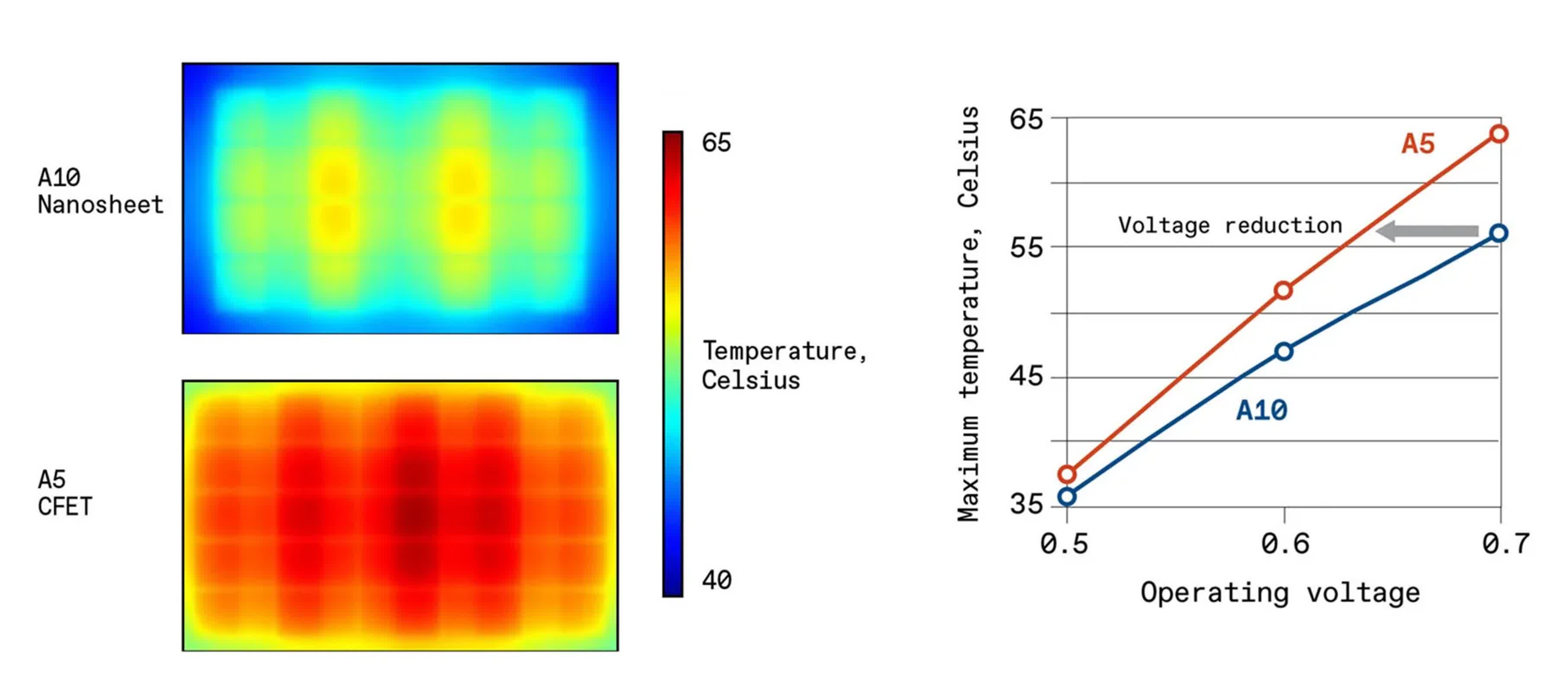
In information facilities housing tens of millions of chips, such a rise in energy density might mark the distinction between secure operation and catastrophic thermal runaway. Conventional cooling strategies, equivalent to air-cooled heatsinks, are already being supplemented by liquid cooling in high-performance services. Nevertheless, even these superior strategies could also be inadequate to handle the warmth generated by the subsequent technology of chip applied sciences.
To deal with this, researchers are investigating different options, together with microfluidic cooling, which channels coolant by way of microscopic passages embedded inside the chip; jet impingement, which makes use of high-velocity coolant streams directed on the chip’s floor; and immersion cooling, the place complete boards are submerged in a thermally conductive dielectric fluid.
But these strategies is probably not sensible in all settings – notably in cellular gadgets the place dimension, weight, and battery life are tightly constrained, or in information facilities the place infrastructure upgrades might be pricey and disruptive.
Past cooling, system-level methods are more and more used to handle temperatures. Thermal sensors, for instance, can set off dynamic reductions in voltage and frequency to decrease energy consumption. Nevertheless, this usually comes on the expense of efficiency, a trade-off acquainted to anybody whose smartphone slows down beneath the warmth of direct daylight.
One other approach, generally known as thermal sprinting, rotates workloads amongst processor cores, permitting overheated cores to chill whereas others take over. Though efficient for brief bursts of exercise, this strategy can scale back total throughput and introduce latency throughout sustained workloads.
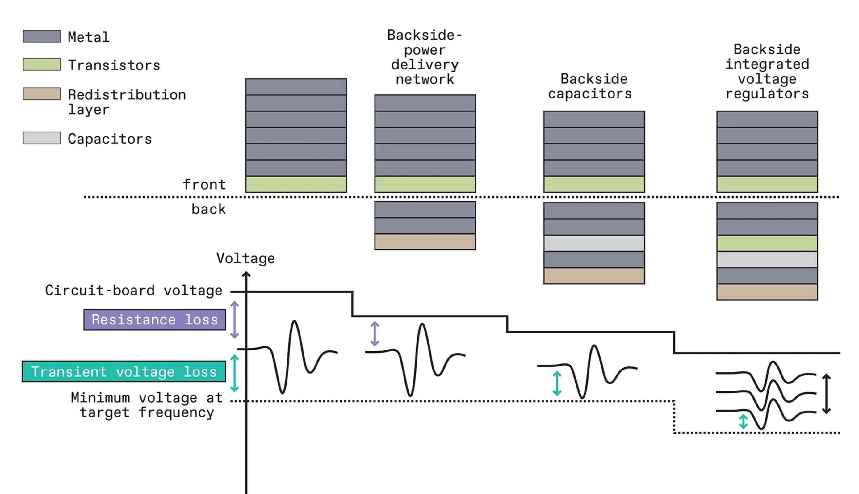
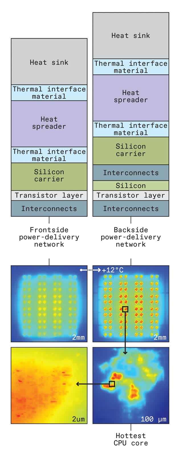
A promising new frontier in thermal administration entails leveraging the bottom of the chip wafer. By relocating the facility supply community to the underside of the chip, a method generally known as bottom energy supply community (BSPDN), engineers can scale back electrical resistance and allow operation at decrease voltages, thereby lowering warmth technology.
All main superior CMOS foundries are anticipated to undertake BSPDN expertise by 2026. Future enhancements could embody integrating high-capacity capacitors and on-chip voltage regulators on the bottom, enabling finer voltage management and additional bettering power effectivity.
These improvements aren’t with out trade-offs. Thinning the silicon substrate to allow bottom applied sciences can scale back its capacity to dissipate warmth, probably creating new thermal scorching spots. Simulations recommend that BSPDNs might enhance native temperatures by as a lot as 14 levels Celsius, highlighting the necessity for added mitigation methods.
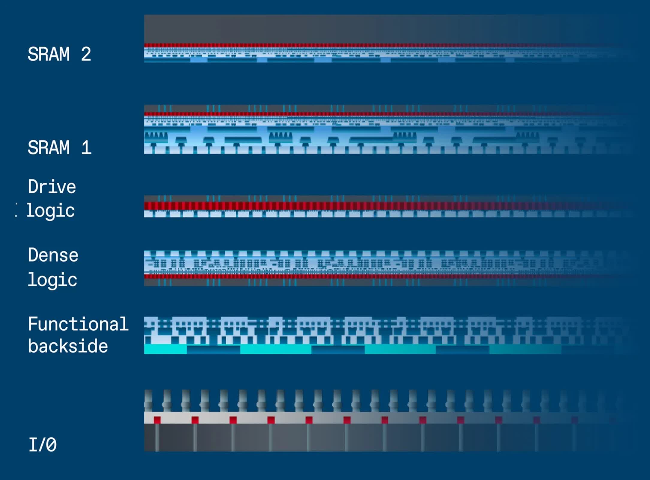
These developments fall beneath what Imec refers to because the “CMOS 2.0” period, which is outlined by superior transistor architectures and specialised logic layers. By optimizing how indicators are pushed throughout the chip, these applied sciences goal to ship improved efficiency and power effectivity alongside potential positive aspects in thermal administration.
Nonetheless, the complete thermal implications stay unsure and demand thorough investigation as these applied sciences proceed to evolve.
Myers warns that software-based approaches to thermal management, whereas helpful, are inherently imprecise. They usually throttle bigger areas of a chip than mandatory, which might unnecessarily scale back efficiency. As an alternative, he advocates for a holistic technique generally known as system expertise co-optimization, which integrates system design, bodily structure, and course of expertise right into a unified improvement course of.
Myers concludes that by fostering collaboration throughout disciplines and leveraging superior simulation instruments, the {industry} can higher anticipate and handle the mounting thermal challenges dealing with future chips.
